Tap Cell Process Diagram Nmos Cmos Implement Nmos Transistor
Example nmos circuit analysis Fabrication nmos steps silicon integrated circuit vlsi circuitstoday Mosfet symbols enhancement mosfets
13: Schematic of measurement setup for I-V extraction of NMOS (top) and
Cmos implement nmos transistors pmos separate Basic structure of t-cell for nmos Fabrication nmos explain silicon substrate
Nmos fabrication: step 1: processing the substrate
Nmos fabrication stepsNmos fabrication process steps Nmos ic technology, cmos ic technologyA: fabrication process of nmos device, steps 1-5 (b) steps 6-9.
In making an nmos transistor using a process similarA: fabrication process of nmos device, steps 1-5 (b) steps 6-9 Nmos principle explanationFigure 3 from fabrication of isfet microsensor by diffusion-based al.

Ohne verbunden serviette transistor mos tennis herrin lol
Tap cell cells well layout placement useCross section of two transistors in a cmos gate, in an n-well cmos Well tap cells in physical designNmos device publication.
Solution: nmos fabrication stepsFast free shipping quality merchandise commodity shopping platform Nmos transistor layout with a deep n-wellElectronics idea: mosfet as a switch.

Vlsi cmos latch cells
Mosfet technology tutorial fabrication mos process nmos pmos cmos13: schematic of measurement setup for i-v extraction of nmos (top) and Analog layoutPmos circuit diagram.
For the circuit diagram in figure 4, the nmos and pmos were fabricatedNmos transistor : cross section, working, circuit & its differences Schematics of the cells in the a) nmos and b) pmos versionFeol, meol, beol ~ techsimplifiedtv.in.

Nmos fabrication process and steps with diagrams,silicon-gate process
Nmos dc mosfetSolved 1- a: describe all the capacitance in an nmos Fabrication nmosLatch-up prevention in cmos logics.
Schematics of the cells in the a) nmos and b) pmos versionWell tap cell Nmos inverter in vlsiFigure 2 from fabrication of isfet microsensor by diffusion-based al.

Solved a. draw a schematic of the cmos circuit using nmos
Nmos transistorSolved explain each step of the fabrication process of nmos .
.


NMOS Fabrication: Step 1: Processing The Substrate | PDF

FEOL, MEOL, BEOL ~ TechSimplifiedTV.in

13: Schematic of measurement setup for I-V extraction of NMOS (top) and

ELECTRONICS IDEA: MOSFET as a Switch

Well Tap Cell | Tap Cell | Use of Tap Cells | Placement of Tap Cell
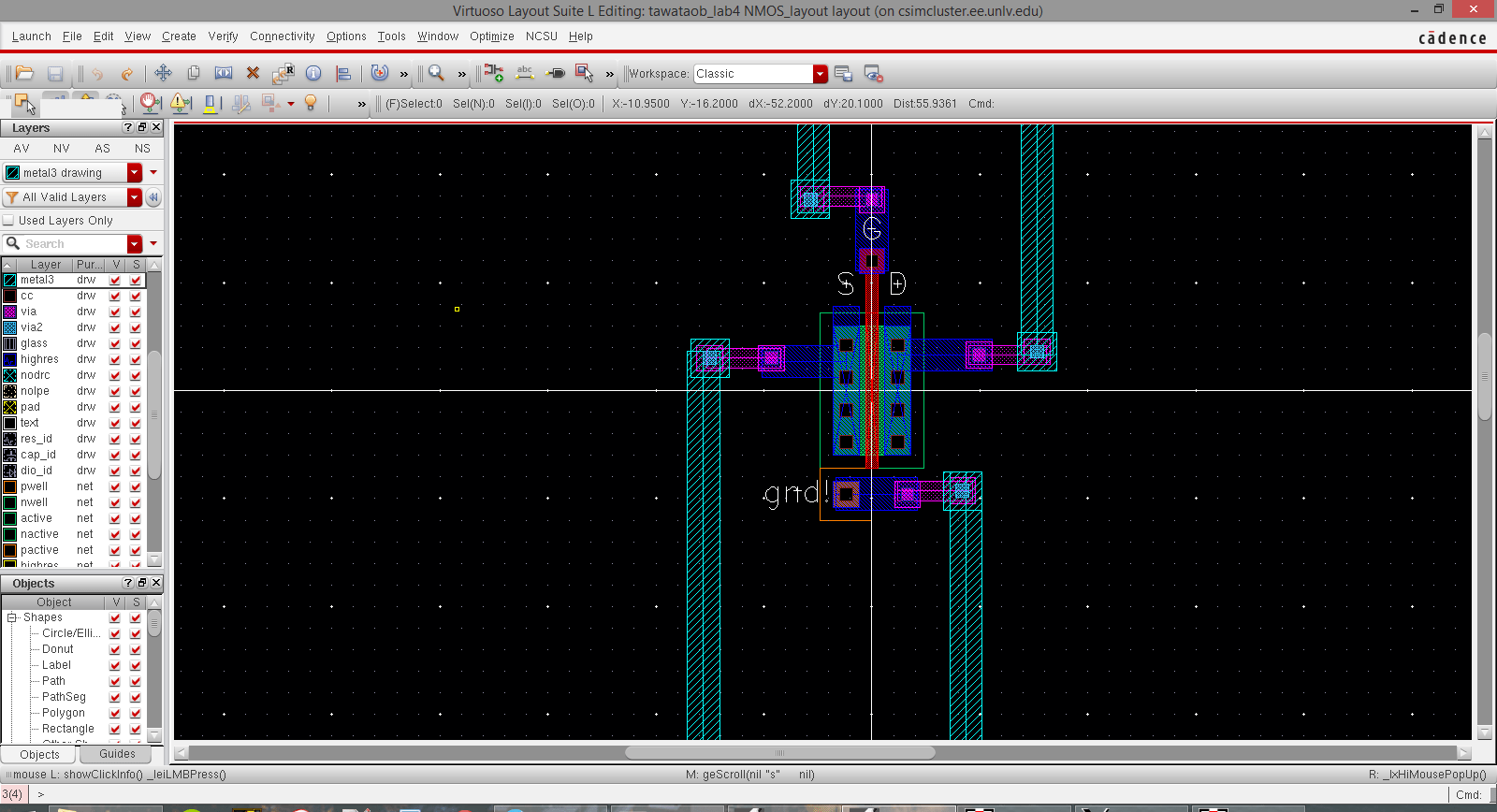
Lab

pmos circuit diagram - Wiring Diagram and Schematics